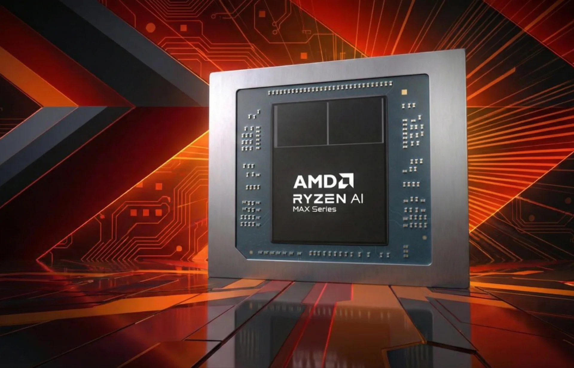
AMD's next-generation flagship Accelerated Processing Unit (APU), rumored to be codenamed "Medusa Halo" and potentially marketed as "Ryzen AI MAX 500," is stirring significant excitement – and some skepticism – in the industry. The biggest headline here is the widespread rumor that Medusa Halo will integrate LPDDR6, the upcoming high-speed memory standard. If true, this positions Medusa Halo as one of the very first System-on-Chips (SoCs) to embrace LPDDR6, promising a radical leap in memory bandwidth and, consequently, a major boost for gaming and AI workloads.
While the tantalizing prospect of this APU hitting the market in late 2027 or by 2028 at the latest keeps us eagerly watching, the devil, as always, is in the details – and the execution.
Medusa Halo: AMD's Vision for Future Performance
As AMD's expected top-tier APU, "Medusa Halo" is rumored to introduce generational upgrades across its entire architecture. This isn't just an incremental step; we're looking at what could be a truly fresh foundation.
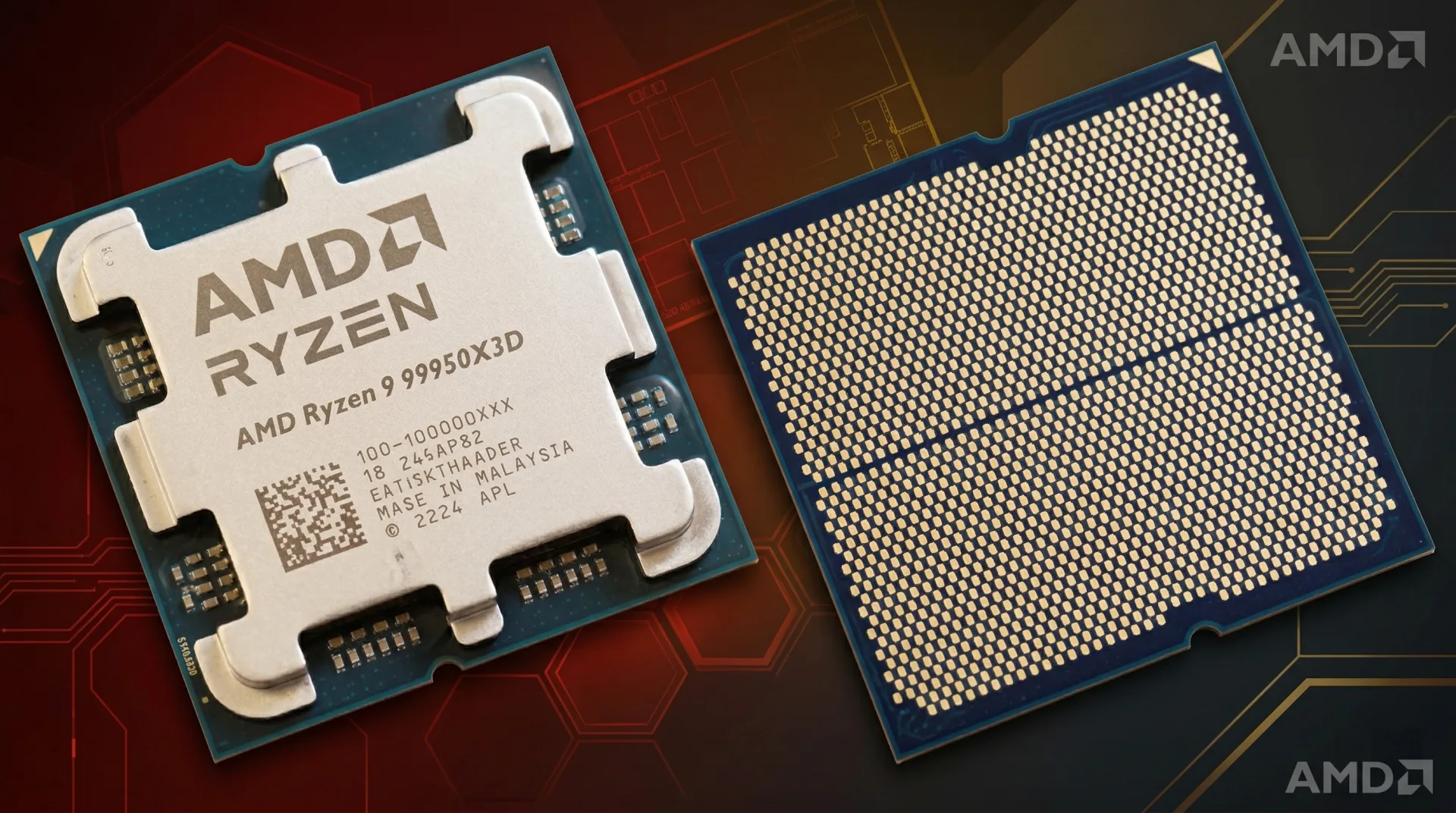
- CPU Architecture: The leaks point to a Zen 6 core design, potentially starting with a base configuration of 14 cores (12 Zen 6 + 2 Zen 6 LP) and scaling up to a formidable 26 cores (24 Zen 6 + 2 Zen 6 LP). AMD's official roadmap confirms Zen 6 processors for 2026 and beyond. We understand Zen 6, codenamed "Morpheus," to be a substantial redesign focused on throughput, featuring an 8-slot dispatch engine and Simultaneous Multi-Threading (SMT). This isn't just more cores; it's a fundamentally different approach to core design, which could lead to significant performance uplifts, particularly in heavily threaded applications. Some community discussions online express hope that this redesign will bring substantial IPC (Instructions Per Cycle) gains, making it a compelling upgrade even for those on Zen 4.
- Manufacturing Process: The CPU chiplets are projected to leverage TSMC's cutting-edge N2P process, while the I/O die may utilize TSMC N3P. This split-node strategy is intriguing. TSMC's N2P process, set for production around Q3 2026, promises an 18% speed improvement at the same power or a 36% power reduction at the same speed compared to N3E. Meanwhile, N3P, already in production since 2024, offers 5% better performance and 5-10% lower power consumption than N3E. This suggests AMD is prioritizing power efficiency and performance density for its core logic, a smart move for an APU designed for a wide array of systems, from laptops to mini-PCs.
- GPU Architecture: The integrated graphics are set to usher in the next-generation RDNA 5 architecture, reportedly packing 48 Compute Units (CUs) and a rumored 20 MB of L2 cache. This is a substantial leap from current integrated solutions.
- AI Technology: The inclusion of next-gen XDNA technology to manage demanding AI workloads, especially Large Language Model (LLM) inference, is entirely expected given the current industry trajectory. We expect this to be a key differentiator, enabling more capable on-device AI experiences.
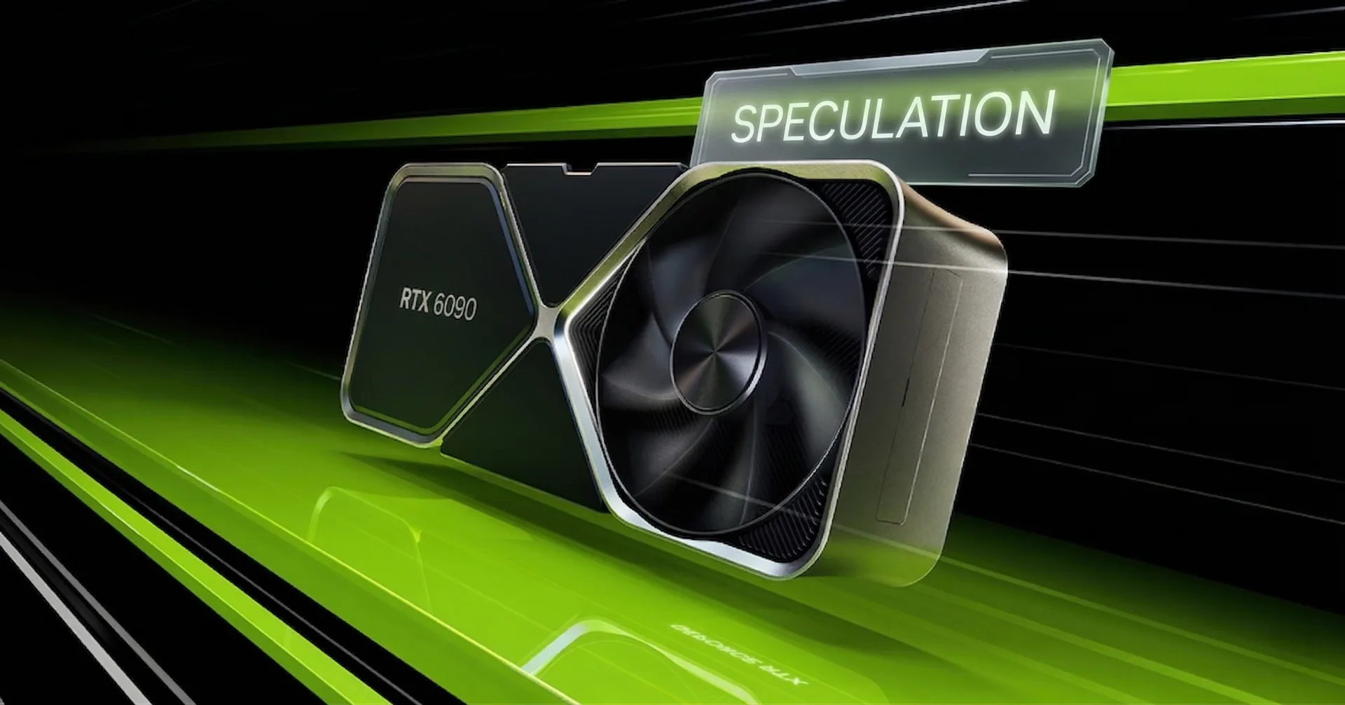
- Performance Targets: Early speculation is aggressive, suggesting Medusa Halo's graphics performance could potentially rival NVIDIA's GeForce RTX 5070 Ti. This would mark a truly remarkable generational upgrade over current "Strix Halo" APUs. However, we approach such direct GPU comparisons with a degree of caution. Dedicated GPUs like the RTX 5070 Ti, released in February 2025 with an MSRP of $750 (though often selling for more), operate in a different power and thermal envelope, and typically feature discrete memory, offering superior sustained performance. While the ambition is commendable, APUs historically face thermal and power constraints that can limit how close they can truly get to discrete graphics in sustained, high-fidelity gaming.
LPDDR6 Memory: The Bandwidth Revolution
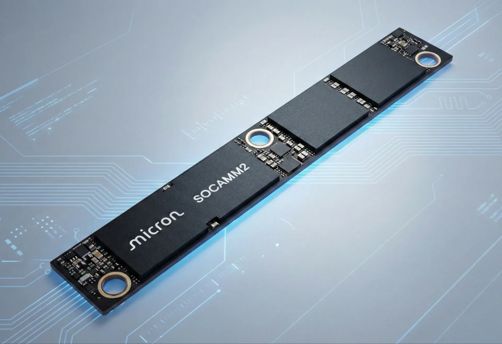
The rumored integration of LPDDR6 memory is, in our view, the most critical element of the Medusa Halo leaks. LPDDR6 represents a significant evolution over LPDDR5X, primarily in speed and bandwidth. JEDEC officially published the LPDDR6 standard in July 2025, defining speeds from 10,667 to 14,400 MT/s. It introduces a dual sub-channel architecture (two 12-bit sub-channels per die, totaling 24 bits per channel), which helps double the effective bandwidth per channel compared to LPDDR5X.
- Speed: JEDEC has confirmed LPDDR6 memory will feature speeds of 14,400 MT/s across a 24-bit wide channel. Innosilicon's LPDDR6 modules already hit an impressive 14.4 Gbps, while Samsung's initial modules achieve 10.7 Gbps. For context, LPDDR5X typically runs at 9.6 Gbps. The jump from 9.6 Gbps to 14.4 Gbps is not just a number; it translates directly into how much data the APU can feed its CPU, GPU, and NPU components.
- Bandwidth Potential: This is where things get exciting. A rumored 384-bit wide LPDDR6 memory controller could enable a theoretical memory bandwidth of 691.2 GB/s. Even with a 256-bit controller, LPDDR6 at 14,400 MT/s is estimated to deliver 460.8 GB/s. This would represent an astounding 80% increase over the current "Strix Halo" APU. Such a significant increase in memory bandwidth is crucial for modern applications, especially those relying on integrated graphics and demanding AI models.
- Architectural Improvements: LPDDR6 introduces a 24-bit wide channel architecture (comprised of two 12-bit sub-channels), changing the I/O organization from the 16-bit channels used in LPDDR5X to improve efficiency and total bandwidth. Its bandwidth with a single 24-bit I/O channel is double that of LPDDR5X with a 16-bit single channel. Beyond raw speed, LPDDR6 also brings lower voltage operation, dynamic voltage/frequency scaling, and enhanced hardware-based security features, making it more power-efficient and reliable for a wider range of applications, including AI in data centers.
Memory manufacturers like Samsung and Innosilicon are reportedly already supplying LPDDR6 modules for validation, indicating that the technology is maturing rapidly towards mass adoption, expected around 2027. Innosilicon is said to be collaborating with TSMC and Samsung to ensure sufficient production capacity for LPDDR6 IP.
The Memory Bandwidth Battleground: Medusa Halo vs. the Competition
The projected memory bandwidth of the Medusa Halo APU with LPDDR6 would position it incredibly competitively against other high-performance platforms, fundamentally changing the landscape for integrated solutions.
- Compared to Strix Halo: The generational leap is stark. AMD's "Strix Halo" APU, recently unveiled at CES, features a 256-bit wide LPDDR5X memory controller supporting 8,000 MT/s speeds for 256 GB/s bandwidth. Even a rumored "Gorgon Halo" refresh might only nudge LPDDR5X speed to 8,533 MT/s, yielding approximately 273.1 GB/s. Medusa Halo's potential 460.8 GB/s (with a 256-bit LPDDR6 controller) or an astonishing 691.2 GB/s (with a 384-bit LPDDR6 controller) would represent a transformative increase, allowing the RDNA 5 iGPU and Zen 6 cores to operate with unprecedented data access.
- Against Competitors: Intel's 'Panther Lake' 12Xe3 SoCs feature LPDDR5X-9600, representing the fastest LPDDR configuration for x86 notebook PCs. While 'Panther Lake' aims for efficiency and can compete with 'Strix Halo' at lower power envelopes, Medusa Halo's projected LPDDR6 bandwidth would clearly pull ahead, even potentially making a 256-bit LPDDR5X version of Medusa Halo competitive against all of Intel's APUs. Apple's M3 Ultra SoC currently achieves an impressive 819 GB/s with its 1,024-bit interface. While Medusa Halo's highest projections come close, Apple's unified memory architecture is a different beast, often praised by the community for its efficiency in handling large AI models. We believe Medusa Halo's LPDDR6 advantage would significantly narrow the performance gap in memory-intensive tasks, making AMD a formidable challenger in high-performance computing, especially for AI PCs.
"Little Halo" and AMD's Broader Strategy: A Calculated Risk?
A smaller variant, the "Medusa Halo Mini" (or "Little Halo"), is also rumored. This APU is aimed at notebooks and compact systems, potentially featuring 14 cores (4 Zen 6 + 8 Zen 6c + 2 Zen 6 LP) and 24-28 RDNA 5 CUs. While primarily supporting LPDDR5X, LPDDR6 support remains a possibility for this chip as well. This tiered approach makes sense for market segmentation.
AMD's current "Gorgon" APUs, like Gorgon Point and Gorgon Halo, are based on Zen 5 CPU and RDNA 3.5 GPU. While Medusa ushers in Zen 6 and RDNA 5, AMD reportedly plans to keep its RDNA 3.5 iGPU long-lived, potentially until 2029. This means many consumers buying laptops in the coming years will continue to experience integrated graphics capabilities similar to today's Ryzen AI 300 and 400 series processors. This strategy is a calculated risk. While it might offer stability and cost-effectiveness for entry-to-mid-range segments, it could also lead to a perception of stagnation if competitor integrated solutions (like Intel's evolving Arc graphics in Panther Lake) continue to improve rapidly. We think AMD needs to clearly articulate the value proposition of RDNA 3.5's longevity to prevent it from feeling like a missed opportunity for mainstream performance uplift.
Our Take: Hopeful, Yet Realistic
It is crucial to note that all information regarding AMD's "Medusa Halo" and "Medusa Halo Mini" APUs, including specifications and performance projections, is based on unconfirmed leaks, rumors, and speculation. AMD has not officially confirmed these products or their specific features. While we are excited by the prospect of an APU pushing such boundaries, these details should be treated with a degree of skepticism until official announcements are made. The rumored LPDDR6 integration and Zen 6 architecture paint a compelling picture for the future of AMD's APUs, particularly for gaming and AI. However, achieving the rumored RTX 5070 Ti-level graphics performance in an APU, while managing power and thermals, remains a significant engineering challenge. We'll be watching closely to see if AMD can turn these ambitious leaks into real-world triumphs.


Comments