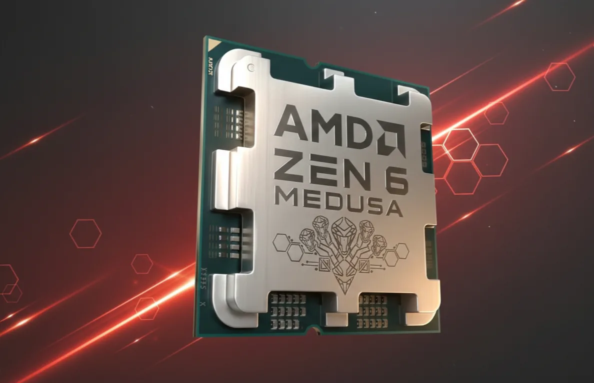
The whispers from the silicon world are growing louder, and they're all pointing to AMD's next-generation Zen 6 CPU architecture, codenamed "Medusa." Recent leaks, reportedly from internal channels, offer an extensive early glimpse into what AMD has planned for its upcoming desktop, server, and mobile processors. These aren't just minor tweaks; we're seeing suggestions of significant architectural advancements, including substantial boosts in core counts and L3 cache, all built upon TSMC's cutting-edge 2nm nanosheet process technology.
Reports indicate a complete ground-up redesign for Zen 6, with AMD reportedly prioritizing multi-threaded performance. It seems early engineering samples of Zen 6 client CPUs are already making their way to partners, with the first products expected to launch in the latter half of 2026. From our perspective, this early partner engagement suggests AMD is confident in its timeline and architectural direction.
Zen 6's Core Density Leap: Beyond Zen 5
The heart of the "Medusa" architecture centers on the standard Zen 6 CCD (Core Complex Die), which is reported to feature an impressive 12 CPU cores and 48 MB of L3 cache. This is a notable 50% increase in both CPU core counts and L3 cache capacity compared to previous Zen 5 CCDs, which typically housed 8 cores and 32 MB of L3 cache. The allocation of 4 MB of L3 cache per core is generous, suggesting a strong focus on keeping data close to the processing units and improving individual core performance.
What's particularly striking is that all 12 cores are said to reside within a single CPU core complex (CCX). The reported die size for this standard Zen 6 CCD is approximately 76 mm². This is a modest 5-7% increase over the Zen 5 CCD's 71 mm² die size, despite the substantial gains in core count and cache. While this efficiency sounds incredibly promising, we remain cautiously optimistic. Achieving such density and performance while maintaining a minimal die size increase is largely attributed to the transition to TSMC's advanced N2 (2nm nanosheet) process node. This will be a true test of the N2 node's capabilities in real-world chip design.
EPYC Venice and Dense Cores: Challenging the Data Center
Beyond the standard Zen 6 CCDs, AMD is also expected to introduce Zen 6C CCDs, designed for higher core density and improved compute performance per watt, likely operating at lower clock speeds. These Zen 6C CCDs will also be manufactured on the TSMC N2 process node.
There are conflicting reports regarding the exact specifications of the Zen 6C CCDs. Some sources suggest they will feature 16 cores and 64 MB of L3 cache per CCD, while other, more numerous reports claim an even denser design with 32 cores and 128 MB of L3 cache per CCD. From our perspective, the 32-core variant would be a more aggressive and impactful play, allowing AMD to truly push the boundaries of compute density in its server lineup.
These Zen 6 and Zen 6C CCDs are set to power AMD's 6th Gen EPYC server processors, codenamed "Venice" (EPYC 9006 series), with an anticipated 2026 launch. EPYC Venice chips are confirmed to be among the first to utilize TSMC's 2nm process technology. These server CPUs are expected to support up to eight CCDs, offering a maximum of 96 Zen 6 'classic' cores (192 threads) or an impressive 256 Zen 6C dense cores (512 threads). This level of scalability could present a serious challenge to Intel's future server offerings like Diamond Rapids and Clearwater Forest, which are also expected around 2026, especially if AMD can maintain its performance-per-watt advantage.
EPYC Venice will introduce new SP7 and SP8 platforms. The SP7 platform will support 16-channel DDR5-12800 memory and up to 600W TDP, while the SP8 will feature 12-channel DDR5-12800 memory with a TDP of 350-400W. Both platforms are anticipated to feature extensive PCIe Gen 6 support, ranging from 128 to 192 lanes. The move to PCIe Gen 6, while perhaps ahead of broad peripheral adoption, ensures these platforms are ready for the next generation of AI accelerators and high-speed storage demands.
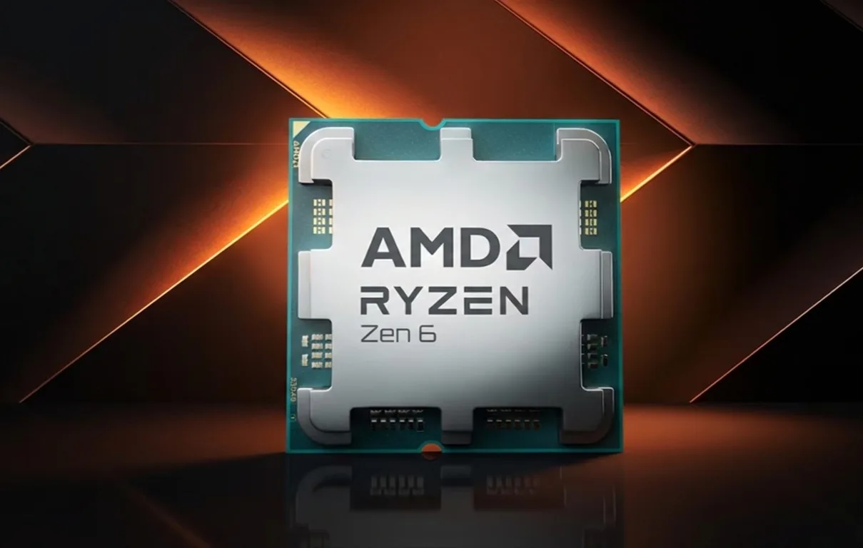
Ryzen Client CPUs: Olympic Ridge and Medusa Ridge's Desktop Battle
For the client desktop segment, the Zen 6 architecture will be branded "Ryzen," with specific client codenames "Olympic Ridge" and "Medusa Ridge". These processors are anticipated in the second half of 2026 and are expected to retain compatibility with the existing AM5 socket, a welcome move for current AMD users.
Zen 6-based Ryzen client CPUs are projected to feature up to 24 total CPU cores (48 threads) in dual-CCD designs. The considerable increase in L3 cache, combined with architectural improvements, is expected to deliver excellent gaming performance and significant gains in both single-threaded and multi-threaded workloads compared to current Zen 5 offerings. This will be crucial for AMD to stay competitive against Intel's planned Arrow Lake Refresh in early 2026 and the subsequent Nova Lake desktop CPUs later that year, which are also rumored to feature large L3 cache expansions.
Furthermore, AMD is expected to launch Zen 6 X3D processors, utilizing its 3D V-Cache technology. These variants could feature an impressive 144 MB of L3 cache per CCD, combining the 48 MB baseline L3 with an additional 96 MB 3D V-Cache layer. This could lead to up to 288 MB of total L3 cache on dual-CCD desktop AM5 processors. From our analysis, this aggressive cache strategy promises a significant boost for cache-sensitive applications and games, potentially solidifying AMD's leadership in the gaming performance segment.
Medusa Point Mobile APUs: A Question of Graphics
Early details have also emerged for Zen 6 mobile APUs, codenamed "Medusa Point". An early engineering silicon (A0 stepping) for a "Medusa Point" part has reportedly appeared on a global customs declaration platform, indicating an FP10 package with dimensions of 25 x 42.5 mm and a 28W TDP. The FP10 package is described as slightly larger than the FP8 footprint used in current mobile parts.
Information regarding the CPU topology of "Medusa Point" APUs is conflicting. One claim suggests a Ryzen 5/7-class APU might feature a 4 Zen 6 performance cores + 4 Zen 6 dense cores + 2 low-power cores (4C + 4D + 2LP) setup. Another claim, for a Ryzen 9-class APU, suggests a topology that might use a 12-core Zen 6 CCD within a larger configuration, potentially resulting in a combined 16C + 4D + 2LP topology. We believe the ability to blend performance and dense cores will be key for power-constrained mobile environments, offering flexibility that traditional monolithic designs often lack. However, the suggestion that these mobile APUs may retain the RDNA 3.5 graphics architecture gives us pause. While RDNA 3.5 is capable, sticking with it for a 2026 launch could see "Medusa Point" fall behind competitor integrated graphics, especially if Intel pushes harder on iGPU advancements with Lunar Lake and Panther Lake in the interim. Community reactions also express some skepticism, hoping for RDNA4 to truly stand out.
New Interconnect Architecture with Silicon Bridges: The Unsung Hero
A significant architectural change in Zen 6 is the reported introduction of a bridge die positioned beneath the CCD and IOD (I/O Die). This silicon bridge fundamentally alters how the CCD and IOD communicate, creating a more efficient inter-chiplet architecture.
This technology, described as a low-cost, passive component manufactured by UMC and packaged by SPIL, aims to increase inter-chiplet bandwidth while decreasing inter-chiplet latencies. AMD has reportedly utilized similar silicon bridge technology, also known as Elevated Fanout Bridge (EFB), in products like the MI200 accelerator and Xbox Magnus. We view this as a crucial, yet often underestimated, innovation. By improving the fundamental communication pathways, AMD can unlock even greater scalability and efficiency for its multi-chiplet designs, ensuring that the performance gains from increased core counts and cache can be fully realized.
TSMC N2 Process: The Foundation of Performance Gains
The widespread adoption of TSMC's N2 (2nm) process node is a cornerstone of the Zen 6 architecture's anticipated performance and efficiency gains. The N2 process node is a significant leap, marking TSMC's first implementation of Gate-All-Around (GAA) nanosheet transistors. TSMC expects the N2 process to provide a 10-15% increase in performance at the same power, a 15% increase in transistor density, and a 25-30% reduction in power consumption compared to the N3E (3nm) node.
While these figures represent the kind of generational improvements we expect, the sheer core and cache density increases in Zen 6, particularly the minimal die size growth for the standard CCD, will be a true test of N2's capabilities. One outlier report suggested Zen 6 CCDs might use TSMC's 3nm manufacturing process; however, the overwhelming majority of information points to the more advanced TSMC N2 (2nm) node. We consider the adoption of N2 essential for AMD to achieve the ambitious targets outlined in these leaks, especially given that TSMC's N2 is expected to see massive demand and offer a more attractive cost structure compared to 3nm.
Ultimately, these extensive leaks paint a potent vision for AMD's Zen 6 architecture. From server behemoths to agile mobile APUs, "Medusa" appears set to deliver a significant generational leap. The consistent theme of increased core counts, dramatically expanded cache, and advanced manufacturing on TSMC's N2 process suggests AMD isn't merely iterating; it's aggressively pursuing architectural redesigns to cement its competitive position. We're eager to see if these early promises translate into real-world performance that lives up to the hype, particularly as 2026 approaches.


Comments