
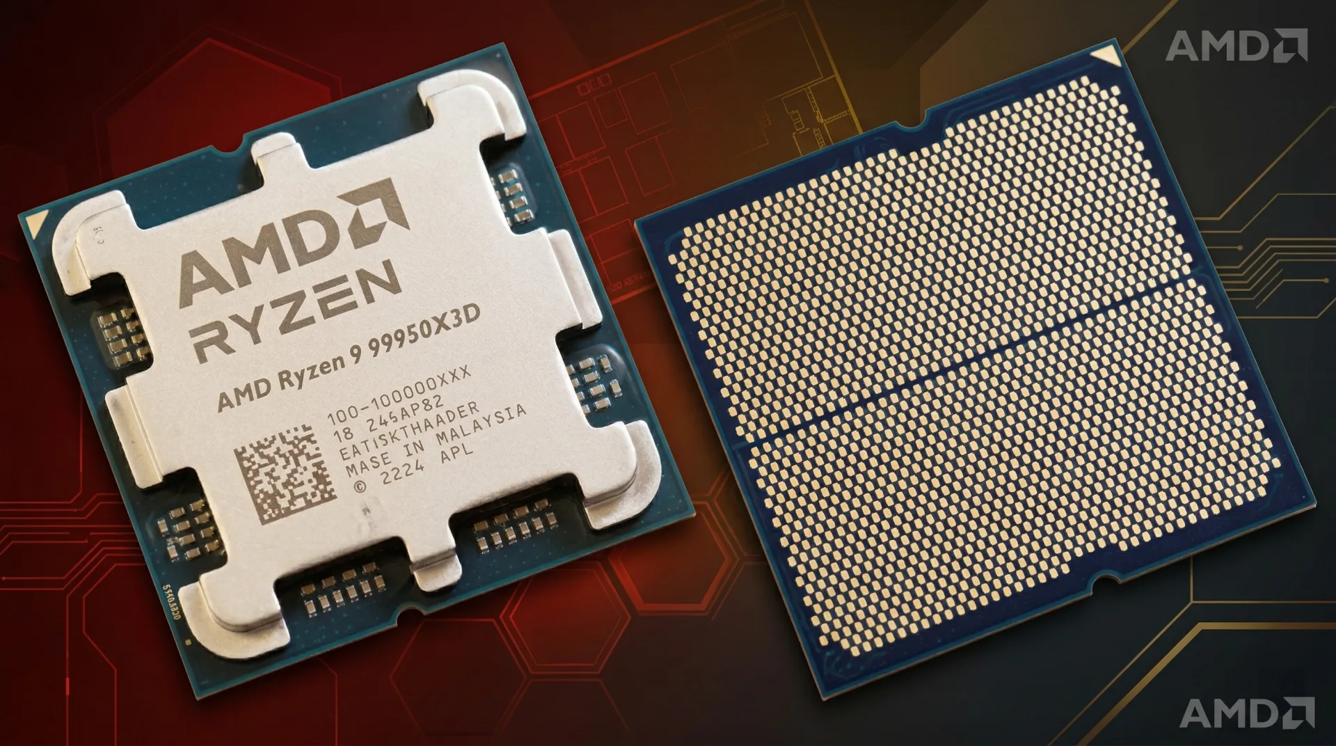
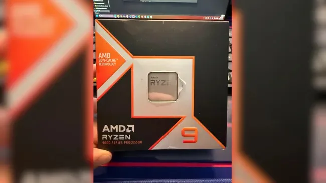
Hardware leaks and official reveals usually follow a predictable rhythm, but ASRock may have jumped the gun on AMD’s next enthusiast flagship. On March 16, 2026, the motherboard manufacturer briefly published a press release on its official website detailing the specifications and support for the Ryzen 9 9950X3D2. While the press release was removed shortly after publication, the details suggest a major shift in how AMD handles its high-end 3D V-Cache architecture.
This is not the first time the "D2" suffix has appeared; it showed up in a Eurasian Economic Commission (EEC) filing back in January. However, the ASRock documentation provides a clearer look at what differentiates this model from the standard 9950X3D that launched last year.
Symmetrical Cache for Both Chiplets
The primary appeal of the Ryzen 9 9950X3D2 is its "Dual 3D V-Cache" configuration. Previous dual-CCD (Core Complex Die) processors, like the 7950X3D and the standard 9950X3D, only featured the extra L3 cache on one of the two dies. This created a two-tiered system within a single CPU: one "gaming" die with the extra cache and one "frequency" die that could boost higher.
Windows and AMD’s drivers had to work hard to ensure games stayed on the cache-heavy die while background tasks or production workloads moved to the faster-clocked die. The 9950X3D2 is designed to resolve this scheduling headache by putting 96MB of L3 cache on both dies, bringing the total to 192MB.
In theory, this should provide more consistent performance across varying workloads, though it comes with a cost in raw clock speed. The 9950X3D2's boost clock is rated at 5.6 GHz—a 100 MHz drop from the 5.7 GHz found on the single-cache 9950X3D.
Ryzen 9 9950X3D vs. 9950X3D2
Thermal and Board Considerations
The increase in cache density and the dual-die 3D V-Cache stack appears to have pushed the power envelope. The 9950X3D2 is rated for a 200W TDP, a notable jump from the 170W of its predecessor.
While ASRock lists support across its entire AM5 stack—from the high-end X870E down to the entry-level A620—that 200W rating should give budget builders pause. Basic A620 motherboards often have modest Voltage Regulator Modules (VRMs) that may struggle to provide steady power to a 200W chip under heavy load. Users on those boards might see the CPU throttle its performance to stay within the motherboard's power limits.
There are also some early reporting quirks. An early CPU-Z validation for the 9950X3D2 reportedly showed only 128MB of L3 cache. This is likely a software limitation; older versions of monitoring tools simply aren't equipped to read the new symmetrical 96MB-per-CCD architecture yet.
Pricing and the Enthusiast Niche
AMD's recent release of the Ryzen 7 9850X3D for $499 showed the company is willing to charge a premium for better-binned parts. There is no official pricing for the 9950X3D2 yet, but given the added complexity of the dual-cache packaging, it is unlikely to be cheap.
For most users, the standard 9950X3D or the 8-core 9850X3D will likely remain the more sensible choices for pure gaming. The 9950X3D2 looks like a specialized tool for enthusiasts who want the 3D V-Cache benefits without the performance "asymmetry" that has defined the 16-core X3D chips until now.
Deployment and BIOS Requirements
- Check your BIOS: If you are planning an upgrade, ASRock indicates that BIOS version 4.03 is required for support. Other manufacturers will likely follow with their own updates soon.
- Power Supply and Cooling: If the 200W TDP holds true, you may need a high-end air cooler or, more likely, a 360mm AIO to keep this chip from hitting thermal limits.
- Wait for Benchmarks: The 100 MHz drop in boost clock suggests that for tasks that don't rely on cache, this chip might actually be slightly slower than the standard 9950X3D. Only direct testing will show if the 192MB of L3 cache makes up for the lower frequency in real-world use.


Comments